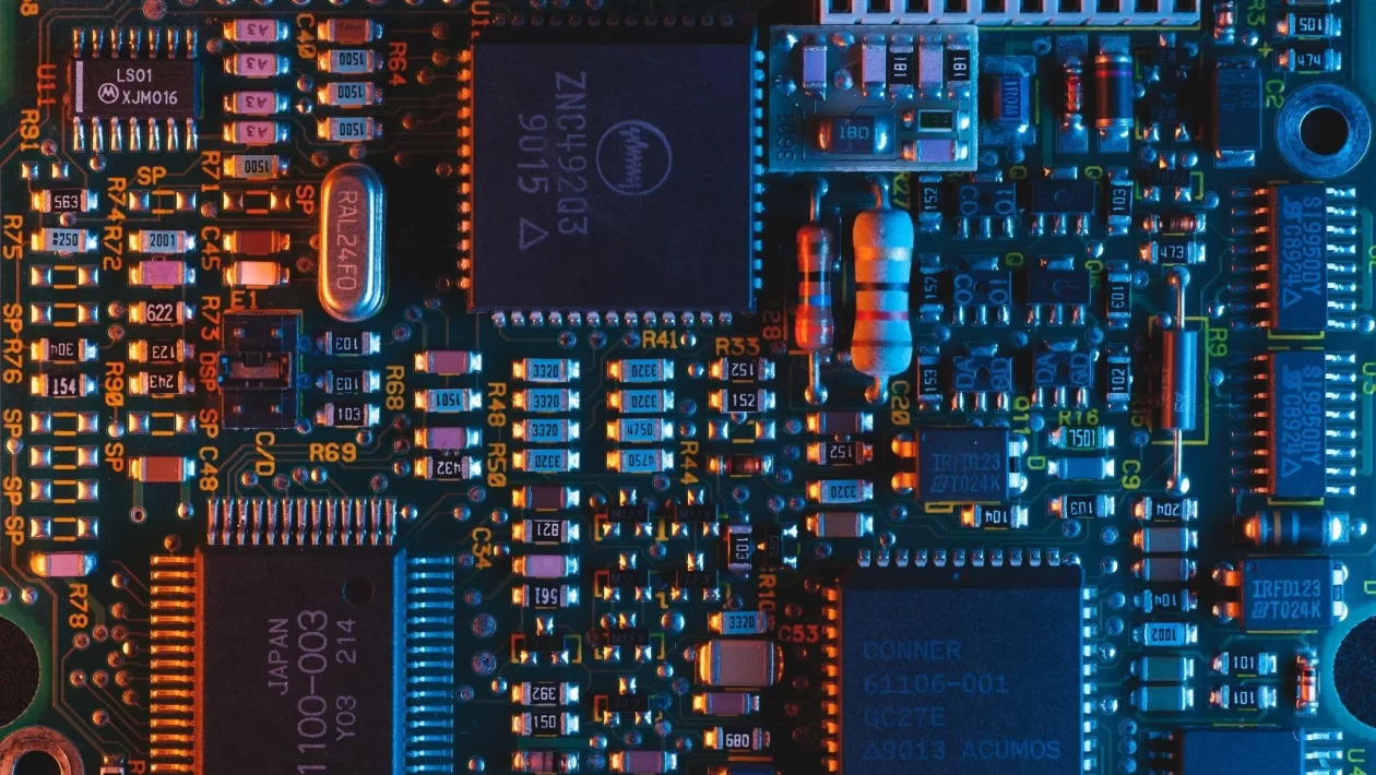
Electronic components, commonly known as surface mounted devices (SMD), are put directly onto the base of a printed electronics board using surface – mounted technology. SMT’s low production costs and tremendous output have made it a hot commodity.
Table of Contents
The term “Surface Mount Technology” (SMT) refers to what?
An electronic component is mounted directly onto a printed circuit board using surface mount technology (SMT), an assembly and manufacturing process. By using this method, more of the assembly work needed to make a functional board may be done automatically throughout the manufacturing process. A surface-mount device is an electrical component that is attached to a circuit board in this way. Direct reflow soldering is used in SMT rather than inserting components via holes, making SMT faster and more convenient than traditional assembly methods.
SMT, which was formerly known as Planar Mounting, replaced Through-Hole Technology and was initially used by IBM in the 1960s in the construction of small-scale computers. It wasn’t until surface-mounted components reached 10% market penetration in 1986 that they really took off. On most modern printed circuit boards, surface-mounted devices (SMDs) had become the norm by 1990.
The SMT components were made with tiny tabs for soldering onto the PCB surface. Components were attached to printed circuit boards via lead holes punched into them during the period of Through-Hole Technology. Click here to read more on printed circuit boards. Device assembly times are drastically reduced by using SMT since it eliminates the need to drill holes on the PCB before soldering on surface-mount devices.
As high-quality SMT assembly demands a great deal of accuracy, the procedure may be time-consuming and laborious if done by hand. Hence, automated assembly machines are often used in SMT production, particularly during high volumes of production, for the sake of efficiency.
Small-form-factor components are far more compact than through-hole components, allowing for the creation of ultra-sleek electronics befitting the present day. This is why SMT is so prevalent now; it can be found in everything from a toy to a laptop to a smartphone.
The Methods Used in SMT Production
Manufacturing using SMT may be broken down into three main phases: printing solder paste, placing components, and reflow soldering. Because of the specifics of SMT manufacturing, however, the following breakdown examines these steps in further detail.
The First Step: Making Your SMC and PCB
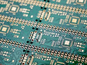
At this early stage, the SMCs and PCBs are chosen and developed. Solder pads are the flat, hole-free areas of copper on the circuit board that are often coated with silver, tin-lead, or gold. In electronic components, such as transistors and chips, the pins rest on solder pads.
The stencil is also essential because it holds the stencil in place so that the solder paste may be printed in the correct locations on the PCB. The quality of these and all other raw materials used in production must be ensured by thorough inspection.
Printing using Solder Paste
At this point, the success or failure of the SMT process hinges. In this step, a squeegee (a printing industry equipment used for cleaning) and the created stencil are used to apply solder paste at an angle of 45° to 60°. Putty-like solder paste (https://en.wikipedia.org/wiki/Solder_paste) is made by combining powdered metal solder with a sticky flux. The flux not only helps clean the soldered surfaces of contaminants and oxidation, but it also acts as a temporary adhesive to keep the surface – mounted components in place.
Instead, solder paste is utilized to join the SMC to the PCB’s solder pads. Make sure the paste is evenly spread throughout each pad. If not, the reflow oven won’t be able to melt the solder enough to create a connection. A reflow furnace is an electrical heating device to use in surface – mounted technology in the devices manufacturing sector to solder electronic components onto circuit boards that are printed.
The Third Step: Organizing the Parts
The next step is to put components on the Board using pick-and-place equipment. The placement machine uses a vacuum or gripper nozzle to extract each component from its package before placing it in its designated spot. The fast and exact machines insert 80,000 electrical components each hour on the PCB, which is conveyed on a conveyor belt. The technique requires precision since reworking a soldered-in mistake may be expensive and time-consuming. This is why any surface mounted device company hires experts in applications for the task.
Reflow Soldering is the Fourth Process in the Sequence
When SMCs are installed, the PCB enters the reflow soldering oven and travels through the following zones:
- In the first part of the oven, called the preheat zone, the circuit board and all its associated components are heated gradually yet uniformly. The temperature is raised to between 140 and 160 degrees Celsius at a pace of 1.0 to 2.0 degrees Celsius per second. Here, in the soak zone, the board will stay hot for 60–90 seconds, with the temperature ranging from 140°C to 160°C.
- After entering the reflow zone, the boards are heated to a maximum of 210°C-230°C, where the tin inside this solder paste melts and the component leads are welded to the patches on the PCB at a rate of 1.0°C-2.0°C per second. The components are held in place by the molten solder’s surface tension.
- The last step is a cooling zone, which ensures the solder solidifies once it leaves the heating zone. These steps, using solder paste or glue to secure the SMCs, may be performed on the other side of the printed circuit board.
Sixth, Inspect and Clean
Cleaning and inspecting the board for defects follows soldering. If flaws are discovered, they are fixed and the product is then put away. Magnifying glasses, automated optical inspection (AOI), flying probe testers, X-ray inspection, etc. are common tools for SMT inspection. Machines are utilized in place of human observers because they provide faster and more reliable findings.